


What is a Semiconductor Technician?

A semiconductor technician is a manufacturing technician who performs the fabrication and testing steps that transform raw silicon into working electronic semiconductors. The semiconductor technician loads semiconductor material into a furnace and saws the formed ingot into segments. Each segment then enters a crystal-growing chamber. X-ray equipment locates the crystal axis before the ingot is sliced into wafers. The wafers pass through cleaning, polishing, and a series of special-purpose furnaces and chemical baths that form the circuitry. Federal occupational data lists the role as semiconductor processor, and industry postings call it wafer fab technician.
Occupational classification is the coding system that assigns the role an official title, a group, and a numeric code. The Occupational Information Network (O*NET) files the role under code 51-9141.00 as Semiconductor Processing Technicians, updated in 2026. BLS, as quoted by Central State University, describes the same coded occupation as work in the manufacturing and testing of microchips used in electronics. The boundary of the code excludes circuit design and sales, since the coded work stops at the fabrication and testing stages of chip production. That boundary shapes what a technician does on every shift.
What Does a Semiconductor Technician do?
A semiconductor technician operates and monitors the fabrication equipment that turns silicon wafers into microchips. The technician executes a process recipe that engineers have written. The recipe fixes the temperature, chemistry, and timing of each step. Each step runs on a tool that the technician loads, starts, watches, and unloads. The tools run etching, deposition, diffusion, and photolithography processes on the wafer, according to the O*NET task list. Watching the tool matters more than touching the wafer, because modern fabs are highly automated. Hands-on work in an automated fab consists of feeding the machines and keeping them running, which protects uptime. Uptime decides the daily output of a fab, since a shutdown costs the plant enormous sums. The boundary of the job ends at the recipe, so a technician never designs chip features or writes circuit layouts. The technician reports equipment alarms and process deviations to the engineer who owns the recipe instead. That reporting line holds for every type of semiconductor technician on the fab floor.
What are the Types of Semiconductor Technician?
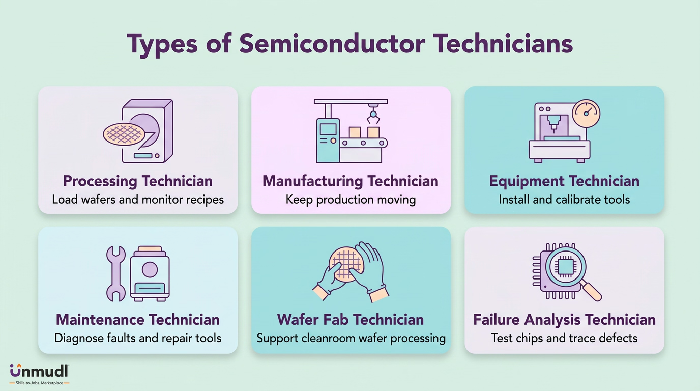
There are six main types of semiconductor technician based on whether the technician handles the wafer, the tool, or the finished chip. The types are semiconductor processing technicians, semiconductor manufacturing technicians, semiconductor equipment technicians, semiconductor maintenance technicians, wafer fab technicians, and semiconductor failure analysis technicians. The table below places the six types side by side on the object handled, the core task, and the employer setting.
| Type | Object Handled | Core Task | Employer Setting |
|---|---|---|---|
| Semiconductor processing technician | Silicon wafer | Loading the tool and monitoring the recipe | Entry point of the fab floor |
| Semiconductor manufacturing technician | Production line | Feeding the machines and clearing alarms | High-volume fab running around the clock |
| Semiconductor equipment technician | Fabrication tool | Installing, calibrating, and servicing the machinery | Fab or tool maker |
| Semiconductor maintenance technician | Faulted tool | Diagnosing the fault and restoring production | Fab with on-call weekend rotation |
| Wafer fab technician | Cleanroom air | Wiping surfaces to a zero-particle standard | Every controlled area of the plant |
| Semiconductor failure analysis technician | Finished chip | Tracing a defect back to its process step | Test and assembly lab |
| Shared across all six | The wafer path through the fab | Executing a recipe an engineer writes | The cleanroom of a fab |
1. Semiconductor Processing Technician
A semiconductor processing technician is a wafer-stage technician who carries silicon through the furnace, saw, bath, and polish steps that form circuitry. The processing technician loads each wafer into the tool, starts the recipe, and monitors the controls until the cycle ends. Monitoring the cycle keeps the wafer inside its process window. Employers treat this role as the entry point of the fab floor.
2. Semiconductor Manufacturing Technician
A semiconductor manufacturing technician is a line-stage technician who keeps the automated production line moving from wafer start to finished chip. The manufacturing technician feeds the machines, changes consumables, and clears alarms so that throughput holds steady across a shift. Steady throughput protects yield, which is measured in wafer starts per day. Employers hire this type for high-volume fabs that run around the clock.
3. Semiconductor Equipment Technician
A semiconductor equipment technician is a tool-stage technician who installs, calibrates, and services the fabrication machinery rather than the wafers inside it. The equipment technician works for the fab or for the company that builds the tool. Serving the tool maker means traveling between customer fabs to commission new machines. Employers value this type for uptime, since a stopped tool halts every wafer behind it.
4. Semiconductor Maintenance Technician
A semiconductor maintenance technician is a repair-stage technician who diagnoses equipment faults and restores the tool to production. The maintenance technician replaces worn parts, cleans process chambers, and performs the scheduled preventive checks that pre-empt faults. Preventing a fault costs less than repairing one. Employers rotate this type through on-call weekends because a fab never fully shuts down.
5. Wafer Fab Technician
A wafer fab technician, also called a semiconductor cleanroom technician, is a contamination-stage technician who protects the wafer from airborne particles. The cleanroom technician wears a full-body bunny suit, follows electrostatic discharge (ESD) protocols, and wipes surfaces to a zero-particle standard. A zero-particle standard matters because one speck ruins the circuitry on a wafer. Employers assign this type across every controlled area of the plant.
6. Semiconductor Failure Analysis Technician
A semiconductor failure analysis technician is a chip-stage technician who tests finished microchips and traces a defect back to the process step that caused it. The failure analysis technician examines wafers under a microscope, runs electronic testers, and records the defect pattern for engineers. The recorded pattern lets engineers correct the recipe before the next lot. Employers place this type in test and assembly labs.
Reading the six types by the object each one handles lets a candidate choose a specialty before taking on the duties of the role.
What are the Duties of Semiconductor Technician?

A semiconductor technician carries six main duties, ordered by the path a wafer follows through the fab. The duties are operating fabrication equipment, monitoring process controls, inspecting wafers for defects, cleaning equipment and wafers, recording production data, and troubleshooting equipment malfunctions. The O*NET record for code 51-9141.00 names the same six activities, from loading material into a furnace to troubleshooting minor equipment malfunctions.
1. Operating Fabrication Equipment
Operating fabrication equipment is the core duty of loading wafers into furnaces, saws, chemical baths, and lithography tools and starting each recipe. The operator sets the controls to the recipe values before the run begins. Correct control settings hold the wafer inside its specification. Supervisors judge a new technician first on this duty.
2. Monitoring Process Controls
Monitoring process controls is the watching duty that reads temperature, pressure, and chemical concentration during a run and corrects any drift. A drift left uncorrected spreads across every wafer in the lot. Catching the drift early saves the lot. Supervisors expect the log to show the reading beside the correction.
3. Inspecting Wafers for Defects
Inspecting wafers for defects is the quality duty performed on wafers and finished chips under microscopes and electronic testers. The inspection separates conforming wafers from scrap before the next step adds cost. Scrap caught early costs less than scrap caught at packaging. An inspection record that reaches an engineer early lets the engineer detect a process error before the next lot starts. Supervisors trace yield loss back through these inspection records.
4. Cleaning Equipment and Wafers
Cleaning equipment and wafers is the contamination duty that scrubs process chambers, polishes wafer surfaces, and swaps filters between cycles. A clean chamber releases no particle onto the next wafer. No particle means no short circuit in the finished chip. Supervisors schedule this duty at every tool changeover.
5. Recording Production Data
Recording production data is the documentation duty of logging recipe parameters, consumable changes, and inspection results for each lot. The log becomes the evidence engineers read when a lot fails. Reading the log locates the failing step within minutes instead of days. Supervisors audit the log at every shift handover.
6. Troubleshooting Equipment Malfunctions
Troubleshooting equipment malfunctions is the repair duty that answers a tool alarm, isolates the fault, and replaces the failed component or escalates it to engineering. A fast response shortens the downtime of the tool. Shorter downtime keeps wafer starts per day on target. Supervisors measure this duty in minutes of lost production.
Carrying out the six duties in sequence keeps a wafer moving from raw ingot to tested chip inside the controlled environment of the fab.
Where does a Semiconductor Technician Work?

A semiconductor technician works inside the cleanroom of a semiconductor fabrication plant, known as a fab. A fab is a large indoor manufacturing facility where microchips are mass-produced under filtered air and controlled temperature. BLS employment data place 94% of semiconductor technicians in the semiconductor and other electronic component manufacturing industry. The remainder work at the equipment firms whose tools serve fabs and at test and packaging operations. The cleanroom inside the fab filters airborne particles, so every semiconductor worker wears a full-body cleanroom garment and never works outdoors. Class-100 or better air filtration is the standard inside an advanced fab. Smaller assembly and test tasks run outside the highest-class cleanroom but still inside a controlled area.
The work schedule of the semiconductor worker is the second condition that the fab sets. Work schedules follow the machines, since a fab operates around the clock in rotating or fixed shifts that cover early mornings, nights, and weekends. Most positions in the occupation are full time, according to the BLS Occupational Outlook Handbook. The station of the semiconductor worker varies between wafer fabrication rooms, chemical processing areas, and test labs. The dry, cool, particle-free air stays the same across all of them. The cool temperature protects the equipment rather than the worker, and the worker stands at a station console for most of the shift. Every worker who enters that air first completes one route of training, credentials, skills, and experience.


